
Recently, Professor Yu Yi's research group from School of Physical Science and Technology, in collaboration with the research team of Purdue University, have made important progress in the research of novel semiconductor heterostructures. For the first time, two-dimensional halide perovskite lateral epitaxial heterostructures have been successfully synthesized and characterized. On April 29, 2020, this research work entitled 'Two-dimensional halide perovskite lateral epitaxial heterostructures' was published online in Nature.
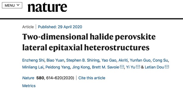
Figure 1. The research work shown on the Nature website
Semiconductors are the physical basis of information technology and form the foundation of modern electronics and optoelectronics. Precise synthesis of semiconductor heterostructures is the starting point of semiconductor engineering. In the past decades, semiconductor materials saw rapid development covering three generations, including elemental semiconductors such as silicon, compound semiconductors such as gallium arsenide, and wide band-gap semiconductors such as gallium nitride. In efforts to satisfy higher demand for future materials science and information science, halide perovskites, a new type of semiconductor material, have attracted worldwide attention in recent years. Halide perovskites show great potential for applications in solar cells, light-emitting diodes and lasers. In particular, being different from traditional covalent semiconductors, halide perovskites have a greater tolerance for lattice mismatch, and therefore have unique advantages in the construction of heterostructures and further large-scale device integration.
On the road to constructing halide perovskite semiconductor heterostructures, there are two scientific challenges. On the one hand, it is difficult to obtain a high-quality atomic-level heterogeneous interface because of high intrinsic ion mobility. On the other hand, microstructure characterization of halide perovskites is challenging as they are so sensitive to air, moisture, and electron beam irradiation, hindering atomic resolution imaging. Lacking guidance from atomic structure information, it is almost impossible to carry out precise design and synthesis of the materials with desired functions.
The Yu Yi’s research team together with the research team from Purdue University, have made a breakthrough in solving these two problems. By introducing rigid organic ligands to inhibit ion diffusion during the synthesis process, they successfully synthesized two-dimensional organic-inorganic hybrid halide perovskite lateral heterostructures. By developing low-dose aberration-corrected electron microscopy, Yu's group revealed the interface of the lateral heterostructure at atomic-scale for the first time, providing evidence of the atomic-level smooth interface obtained. The organic-inorganic hybrid materials are the most electron-irradiation sensitive ones in the family of halide perovskites due to the existence of organic components which bring great challenges to high-resolution structural analysis. The atomic resolution imaging of two-dimensional organic-inorganic hybrid halide perovskites has never before been achieved. In terms of the imaging of radiation-sensitive materials, one effective method should be biological cryo-electron microscopy which was recently awarded the Nobel Prize in Chemistry in 2017. However, biological samples are among the most radiation-sensitive materials, and the two-dimensional organic-inorganic halide perovskites are even more sensitive as they are only several nanometers in thickness rendering the interatomic binding force much weaker. Thus the use of either biological cryo-electron microscopy or aberration-corrected electron microscopy to investigate the atomic-scale structure analysis of these low-dimensional halide perovskites is quite challenging.
Yu’s team developed low-dose aberration correction electron microscopy to tackle this problem. After years of hard work they discovered an optimized low-dose imaging method to study the radiation-sensitive semiconductor heterostructures, and the atomic structural analysis has been demonstrated for the first time. This breakthrough, providing accurate information on the interface atomic structure, defect configuration, and lattice strain, serves as the most intuitive guidance for designing the microstructure of halide perovskite heterostructures. On this basis, the research team further demonstrated the rectification effect in a prototype device, showing the potential application of these novel semiconductor materials.
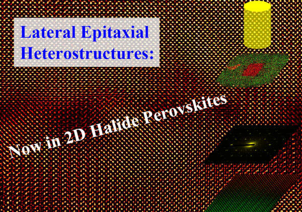
Figure 2. The high-resolution transmission electron microscopy image of the heterostructure interface.
The electron microscopy work was done at The Centre for High-resolution Electron Microscopy (CħEM), which is an advanced electron microscopy platform led by the director, Prof. Osamu Terasaki. Yuan Biao, a PhD student from Yu’s research group, took advantage of the microscopy center and performed most of the microscopy work in this research. “ShanghaiTech is a young university and this research center, CћEM, is happy to support challenging and educational projects whose outcomes will meet the expectations of society in the future. I would like to congratulate our excellent CћEM staff on Prof. Yu Yi and his PhD student Yuan Biao’s success in achieving world top-level research results” Prof. Osamu Terasaki said.
In this study, Dr. Shi Enzheng (postdoctoral researcher, Purdue University) and Yuan Biao (PhD student, ShanghaiTech University) are the co-first authors. Prof. Dou Letian (Purdue University), Prof. Brett Savoie (Purdue University) and Prof. Yu Yi (ShanghaiTech University) are the co-corresponding authors. Material synthesis and molecular dynamics simulation were completed by the Purdue team, and atomic-scale microstructure analysis was performed by Yu Yi’s team at ShanghaiTech University. In addition, research teams from Massachusetts Institute of Technology and University of California, Berkeley also contributed to this work. This work was supported by the startup funding from ShanghaiTech University, the National Natural Science Foundation of China, the Centre for High-resolution Electron Microscopy (CћEM) of ShanghaiTech University, and the Natural Science Foundation of Shanghai.
Article link: https://www.nature.com/articles/s41586-020-2219-7

Yu Yi, Assistant Professor, Principle Investigator (PI)
School of Physical Science and Technology, ShanghaiTech University
The research direction in Yu Yi’s Group is the application of aberration-corrected electron microscopy on microstructure analysis. So far, Prof. Yu has published more than 60 papers and was cited more than 5,000 times.

Yuan Biao, Class of 2022 PhD student
School of Physical Science and Technology, ShanghaiTech University
“Under the guidance of the instructor and senior group members, I became familiar with the electron microscope and understood the principle behind it. Thus, I was able to explore the unknown with courage. Many thanks to the first-class experimental platform provided by ShanghaiTech University, the instructor for careful guidance, the group members for encouragement, and the engineers of CħEM for enthusiastic help!
Figure 3. The Yu Yi’s Group photo taken in 2019